
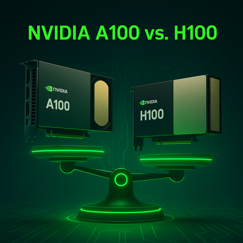
The NVIDIA A100 (Ampere) and H100 (Hopper) are datacenter GPUs built for AI/HPC, but they differ greatly under the hood. The H100’s Hopper GPU is manufactured on TSMC’s 4N (≈5nm) process with ~80 billion transistors, compared to A100’s 7nm GA100 chip with ~54B. The Hopper GH100 chip packs 144 streaming multiprocessors (SMs) with 128 FP32 CUDA cores each, giving up to 16,896 FP32 cores on the full SXM module, whereas A100’s Ampere GA100 has 108 SMs × 64 cores = 6,912 FP32 cores (80 GB SXM). Hopper also increases the number of Tensor Cores (4th gen) to 528 per GPU (versus 432 3rd-gen Tensor Cores on A100).
These hardware boosts translate to far higher raw throughput. For example, an A100 80 GB SXM delivers about 19.5 TFLOPS FP32 (312 TFLOPS with sparsity) and 9.7 TFLOPS FP64. By contrast, the H100 80 GB SXM can do ~60 TFLOPS FP32 and 30 TFLOPS FP64 – roughly 3× more on each metric. Even bigger gains come with new data types: H100’s Transformer Engine adds native FP8 math, giving up to 4× the multiply-accumulate rate of A100 on equivalent workloads (2× for standard 16-bit vs. A100). In practice, NVIDIA reports H100 Tensor Cores deliver 9× faster AI training and 30× faster inference on large language models compared to A100.
Key spec comparisons (80 GB SXM variants) are summarized below:
| Specification | NVIDIA A100 (Ampere) | NVIDIA H100 (Hopper) |
|---|---|---|
| CUDA Cores (FP32) | 6,912 | 16,896 |
| Tensor Cores | 432 (3rd gen) | 528 (4th gen) |
| FP32 Performance (TFLOPS) | 19.5 (312 w/ sparsity) | 60 (990 w/ sparsity) |
| FP64 Performance (TFLOPS) | 9.7 | 30 |
| FP8 Performance (TOPS) | — | 4,000 (sparse) |
| Memory | 40 GB or 80 GB HBM2e | 80 GB or 94 GB HBM3 |
| Memory Bandwidth | 2.04 TB/s | 3.35–3.9 TB/s |
| Tensor Float32 (TF32) | 312 (624 w/ sparsity) | 990 (1,980 w/ sparsity) |
| NVLink Bandwidth | 600 GB/s (NVLink 3) | 900 GB/s (NVLink 4) |
| MIG Instances | Up to 7 (5–10 GB each) | Up to 7 (10–12 GB each) |
| Max Power (TDP) | 400 W (SXM), 250–300 W (PCIe) | 700 W (SXM), 350 W (PCIe) |
A100 supports multi-instance GPU (MIG) with up to 7 partitions (each as small as 5–10 GB). H100 has second-generation MIG (up to 7 slices, with ~10–12 GB each) plus built-in confidential-computing features. In summary, Hopper’s SM delivers roughly 2× the raw compute per SM (and 4× with FP8) of A100, along with specialized Transformer Engine and DPX instructions for AI/HPC. The architectural leaps give H100 an order-of-magnitude advantage for large-scale AI (e.g., NVIDIA expects ~9× training speedup and 30× inference speedup on massive language models).
Performance: Training and Inference
Benchmarks confirm H100’s lead on AI workloads. In MLPerf Training (AI model training) and real-world large-model training, H100 clusters train models much faster than A100 clusters. For instance, NVIDIA reports an 8×8 A100 cluster training GPT-3 (175B) in ~28 minutes, whereas 8×8 H100 (SXM) cuts that time to ~7 minutes (roughly 4× speedup). In massive multi-node tests, H100-based systems achieve near-linear scaling; e.g., a 512-GPU H100 system reached GPT-3 training in ~30 minutes in mid-2023, and this has since improved to ~3.4 minutes on 11,616 GPUs (demonstrating ~3.2× perf gain year-over-year at 512-GPU scale). In contrast, equivalent-scale A100 runs took several hours.
For inference and smaller models, H100 also shines due to its FP8 Transformer Engine and huge memory. Independent tests find H100 often delivers 1.5–2× the inference throughput of A100 on large NLP models. For example, one study reports ~130 tokens/sec for a 13B–70B LLM on an A100, versus ~250–300 tokens/sec on an H100. This means an H100 can serve nearly twice the requests per second of an A100 in large-model inference. The gap is narrower in computer vision or smaller models (e.g., ResNet inference might only be ~20–30% faster on H100), but H100 still leads across the board.
NVIDIA’s MLPerf results reflect this: the H100 holds all-training and all-inference performance records in MLPerf 4.0/5.0, consistently outpacing the A100 on every benchmark. In high-performance computing (HPC) workloads, H100-equipped clusters achieved up to 16× faster training than Ampere-era systems over three years. In practical terms, Hopper’s improvements (FP8, NVLink 900GB/s, DPX, etc.) translate to ~2–3× higher performance for most AI tasks, with even larger gains on transformer models.
Memory and Bandwidth
The A100 originally came in 40 GB or 80 GB HBM2/HBM2e configurations. The H100’s initial 80 GB PCIe card also used HBM2e (2 TB/s bandwidth), but the SXM form factor was upgraded to HBM3. A100’s 80 GB SXM delivers ~2.04 TB/s memory bandwidth, whereas H100 SXM can provide ~3.35 TB/s (80 GB HBM3) up to 3.9 TB/s (94 GB HBM3 in the NVL card). In short, H100 offers up to ~1.7× the memory bandwidth of A100. The maximum memory capacity also rises from 80 GB (A100) to 94 GB (H100 NVL) per GPU. This extra bandwidth and capacity allow larger batch sizes and model reservoirs, which are crucial for large LLMs and data-intensive tasks. Both GPUs support NVIDIA’s NVLink for GPU-to-GPU interconnect: A100 uses NVLink 3 (600 GB/s aggregate per GPU pair) while H100 uses NVLink 4 (900 GB/s) and optional NVLink Switch for massive clusters.
Power and Efficiency
H100’s performance gains come with higher power usage. An A100 SXM has a 400 W TDP (and 300 W for the 80 GB PCIe card), whereas H100 SXM draws 700 W and the PCIe card 350 W. These higher power/thermal requirements mean H100 SXM cards need liquid cooling. The upshot is that H100 is physically much hotter and thirstier than A100: e.g., 8×H100 SXM in a DGX A100 rack consumes ~5.6 kW vs ~3.2 kW for A100.
Despite the higher wattage, H100 often offers better energy efficiency (performance per watt) on large AI workloads. Because H100 can do roughly 3× the work per GPU, its per-watt throughput is still significantly higher. Vendors note that H100 yields more operations per watt for high-throughput training than A100. This trade-off must be weighed in deployments sensitive to power: H100 runs hotter but can finish jobs much faster. Overall, H100 is a higher-power GPU that achieves greater total compute density per rack, while A100 is more modest in power (passive-cooled 250–400 W) and easier to fit in older datacenters.
Compatibility with Frameworks
Both A100 and H100 are fully CUDA-compatible accelerators. They work with all major AI frameworks—PyTorch, TensorFlow, JAX, etc.—via NVIDIA’s CUDA and cuDNN libraries. NVIDIA’s AI-optimized software (Magnum IO, cuBLAS, Triton Inference Server, TensorRT, etc.) supports both GPUs. Because H100 is newer, some frameworks have since added FP8 and Transformer Engine optimizations, but code written for A100 will generally run on H100 with no changes (just faster). The MIG feature on each GPU allows partitioning into up to seven independent instances, which both HPC clusters and cloud providers use to share the card among jobs. In practice, any software on an A100 can run on H100. H100 accelerates it more.
Pricing and Availability
A100 and H100 have different price/performance profiles. The A100 80 GB SXM launched around $11–12K by 2024, the market saw ~$18–20K for brand-new units. The H100 80 GB PCIe/SXM launched closer to $25K per card. Thus, H100 typically costs ~25–50% more upfront (ignoring mult-GPU system discounts). Cloud pricing reflects this premium: for example, an AWS p4d (8×A100) instance runs $32/hr ($4.10/GPU), whereas AWS p5.48xlarge (8×H100) is $98/hr ($12.3/GPU). Even on Azure, an H100 VM is ~$6.98/hr per GPU versus ~$3.40 for A100. (Some niche providers offer cheap spot/marketplace rates as low as $2–3/hr per H100, but mainstream pricing is much higher.)
Availability has also evolved. The A100 has been on the market since 2020 and is widely stocked by OEMs and cloud vendors. The H100 debuted in 2022 and was initially scarcer and allocated to large customers. By 2025, supply has improved and even cloud spot offerings for H100 are common, causing its rental price to fall. Many organizations now adopt hybrid strategies: using A100 instances for general workloads or when budgets are tight, and H100 for the most demanding AI projects. One analysis notes that H100’s falling cloud prices erode A100’s cost advantage, making H100’s superior performance (often 2–3× faster on key workloads) a compelling tradeoff. In short, H100 is today a premium GPU (both purchase and rental prices are higher), but its performance gains often justify the cost for large-scale AI projects.
Ideal Use Cases
NVIDIA A100 GPUs remain excellent for a wide range of AI and HPC tasks, especially where cost, compatibility, or existing infrastructure are considerations. Use cases include general ML training (smaller to medium models), HPC workloads already optimized on Ampere, inference deployment (especially with MIG and multi-tenant servers), and mixed workloads in data centers with Ampere clusters. A100’s mature ecosystem and slightly lower power make it a safe choice for “steady-state” acceleration. It also shines in environments where MIG partitioning is heavily used to amortize GPU cost across many users.
NVIDIA H100 is targeted at cutting-edge AI and exascale HPC. It excels at training massive transformer models (large language models, multimodal generative AI, etc.), high-fidelity simulations, and any workload that can leverage its FP8/Transformer Engine or vast memory bandwidth. For example, H100 is ideal for companies training state-of-the-art LLMs from scratch or running extensive NLP inference services with minimal latency. Its NVLink/Switch support suits the most significant GPU clusters (thousands of GPUs working in sync). H100 also benefits vision, recommendation, and scientific workloads that can use its increased FP32/FP64 throughput and DPX instructions (e.g., genomics, protein folding, routing). In summary, if your workload is memory-bandwidth-bound or tensor-math-intensive (especially transformers), and budget permits, H100 is the better choice. If your needs are more modest in scale or you require maximum economy and compatibility, the A100 remains a solid workhorse.
In practice, many organizations use both — a “hybrid” strategy leverages A100s for cost-sensitive or legacy workloads and H100s for next-generation AI. Because NVIDIA’s software stack spans both architectures, the transition is straightforward. The key decision factor is often performance-per-dollar: H100 can complete a job in half the time of A100, which may offset its higher hourly cost (as H100’s users have observed). Ultimately, the choice depends on workload characteristics: use H100 when every ounce of AI throughput matters, and A100 where solid acceleration and broader deployment are