

Every time Intel announces a new CPU generation, tech enthusiasts around the world rejoice, looking forward to increased performance, lower power consumption, and cutting-edge features. But despite all the attention new CPU generations receive, most people don’t know how they differ from older generations, and this article is here to fix that.
Every Nanometer Counts
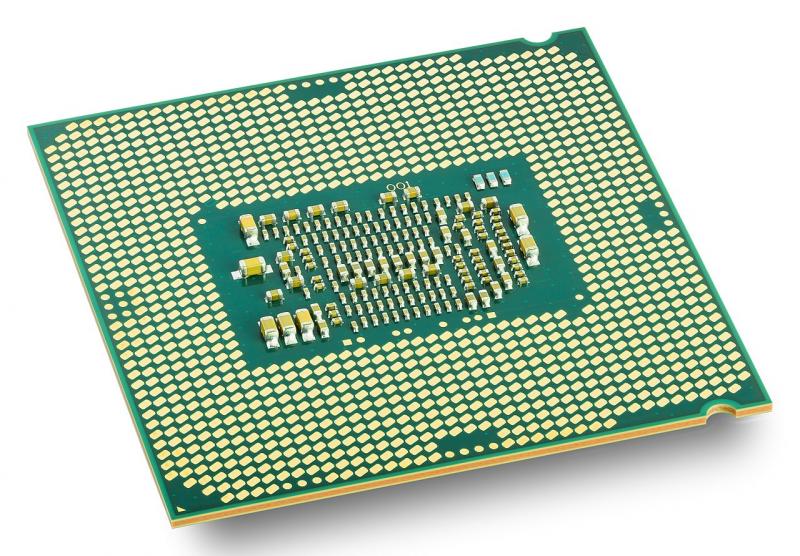
Modern CPUs are manufactured using a process called semiconductor device fabrication. This process consists of multiple complex steps during which electronic circuits are gradually created on a silicon wafer made of pure semiconducting material. It can take up to 4 months from the start of the manufacturing process to a finished CPU being ready for shipment.
Over the years, Intel and other manufacturers have greatly improved semiconductor device fabrication. In 1971, the smallest transistors Intel could manufacture for its Intel 4004 processor measured 10 μm (micrometers). Recently, Intel has announced the 10th generation of its Core processors, called Intel Ice Lake, which is expected in late 2019 and will be based on a new 10 nm (nanometer) architecture.
Why does transistor size matter so much? Because the more transistors a processor has, the more complicated instructions it can perform. In other words, the greater the number of transistors is, the better the performance you can expect.
The Intel 4004 processor from 1971 has just 2,300 transistors. The recently announced Intel Ice Lake CPUs will have billions of them. It would be impossible for manufacturers like Intel to create CPUs with billions of transistors if it weren’t for the advancements in semiconductor device fabrication, because the silicon wafers would have to be enormous, which would make them prohibitively expensive.
Making Chip Packages Smaller
As we’ve explained in the previous chapter, it’s better for CPU manufacturers to figure out how to fit more transistors on a silicon wafer of the same size, which is why some new chips from Intel are going to take advantage of a state-of-the-art 3D stacking technology the company is calling Foveros.
This technology essentially allows Intel to stack complex logic dies on top of one another, providing much greater flexibility to mix and match processor components. A similar technology, called High Bandwidth Memory (HBM), is already in use by graphics card manufacturers, enabling them to achieve high bandwidth through thousands of interconnects between the graphics card and its memory.
“Foveros paves the way for devices and systems combining high-performance, high-density, and low-power silicon process technologies,” explains Intel on its website. “Foveros is expected to extend die stacking beyond traditional passive interposers and stacked memory to high-performance logic, such as CPU, graphics and AI processors for the first time.”
Conclusion
Intel has been perfecting semiconductor device fabrication since it released its first commercially available microprocessor in 1971. With the 10th generation of Intel Core processors upon us, we can see how much CPUs have improved over the years, and we hope that you can now appreciate the technology behind them.